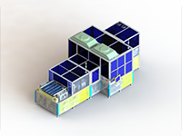
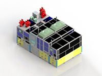
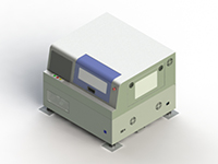
iEHD PRINTER
iEHD PRINTER
-
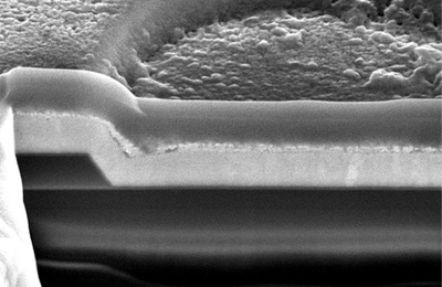
LCD Repair
- ·The open defect is directly repaired by printing metal ink and can achieve high resolution and high quality electrodes.
- ·Compared with the existing CVD repair-technology, the process can allow high resolution patterns and enhanced step coverage and flexibility.
PATTERN SIZE3μm or more
-
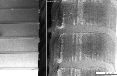
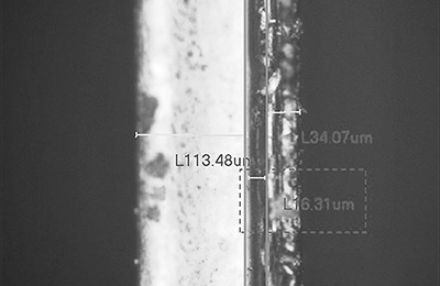
OLED Repair
- ·The open defect is directly repaired by printing metal ink and can achieve high resolution and high quality electrodes.
- ·It can repair 1μm-level patterns, which is the World champion performance.
PATTERN SIZE1.5μm or less
-
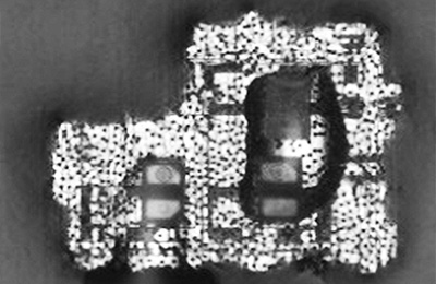
uLED Repair
- ·For the defect free micro-LED display, due to the limit of multi-transfer, repair solution is key process in manufacturing. Enjet provides the chip repairing solution for the micro-LED display.
PATTERN SIZE10μm or less
-
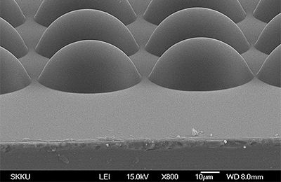
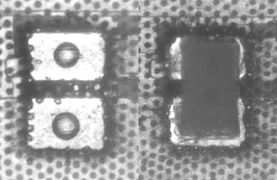
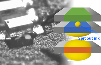
Micro-Precision Bump Printing
- ·Uniform and small features can be printed, which can be less than 10um. It can be applied to bumper fabrication.
PATTERN SIZE10μm or less
-
Underfill
- ·Enjet develops innovative underfill solutions for semi-conductor packaging, based on our dispensing technology.
- ·Compared with the conventional method, due to the effect of the electric field, it has the advantage of void-free underfilling performance.
-
Side Electrode printing
- ·3D edge side electrodes can be successfully fabricated by our solution.
model
-
Bonding & Sealing
- ·Our dispensing technology is being applied to various application areas such as adhesive bonding and sealing.
model

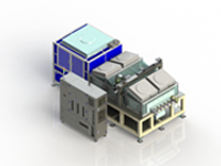
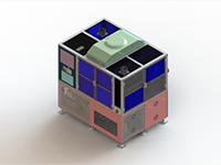
iEHD COATER
iEHD COATER
-
Anti Glare
- ·Enjet has developed solutions for AG coating and applied to customers. EHD spray method can fabricate more uniform films and high yield performance compared with other methods.
-
Anti Finger coating
- ·Anti-finger coatings have been used in many applications such as mobile phones, glasses and displays.
- ·Compared with air and ultrasonic spary coatings, EHD spray coatings can reduce the material usage and achieve a uniform thin film.
-
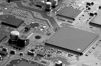
Electromagnetic Interference (EMI) Shielding
- ·The EHD spray method has been applied to the electromagnetic (EMI) shielding of semiconductors and could achieve highly uniform coating layers on 3D chip structure.
-
Conformal Coating
- ·There are many requirements for forming thin films in PCB, chip, display, mobile phones, etc.
- ·Recently, the EHD electrostatic spraying method can uniformly coat the functional materials on entire exposed surfaces of the 3D structure.
model
-
Flux Coating
- ·Flux coating is applied to the surface of the printed wiring board (PWB) or printed circuit board (PCB) before soldering to ensure good adhesion between the solders.
- ·The flux can remove oxide layers, prevent the formation of oxide layers, and improve the quality of the soldering and the electromechanical connection at the interface with the circuit.
- ·EHD spraying methods can carry out thin and uniform coatings for flux applications.
model
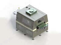
PLASMA
PLASMA
-
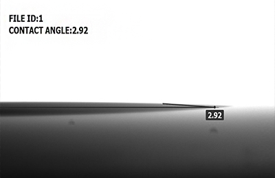
Hydrophilic
- ·ENJET has developed Direct RF plasma head technology with high-density plasma capability and applied it to ultra-precision coating machines for many years.
- ·ENJET's plasma solution can stably ignite plasma and carry out the surface treatment at a long distance.
model
-
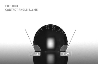
Hydrophobicity
- ·Enjet plasma solution can form a hydrophobic film layer on many surfaces such as wafers, ceramics, and glasses in seconds to minutes.
model
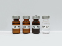
INK
INK
-
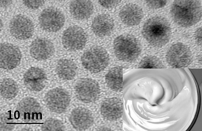
Particle-free conductive ink for Bonding
- ·Product : Micro LED
- ·Target : Anode/Cathode Electrode Based on TFT
- ·Pattern Requirement : < 15 ㎛ diameter
model
-
Particle-free conductive ink for electrodes repair
- ·Product : Micro LED
- ·Target : Data Electrode repair
- ·Pattern Requirement : Edge-Electrodes
- ·Repair Efficiency : 100 %
model
-
Hybrid conductive ink for fabricating electrodes
- ·LERProduct : Micro LED, LCD TV TFT gate/source electrodes
- ·Target : Electrode fabrication
model
-
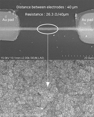
Particle conductive ink for 3D electrodes formation
- ·Direct patterning of edge-electrode using our EHD printer and particle conductive ink
model
-
Particle conductive ink for TFT electrodes formation
- ·High resolution direct patterning of OLED TFT electrode based on nano-particle conductive ink
model
-
Underfill ink for Mini-LED
- ·Thermal curing ink of epoxy base for EHD
- ·Curing temp. 150~200℃/30min
- ·Hard type
model
-
Insulation coating for Micro-LED
- ·Thermal curing ink of epoxy base for EHD
- ·Low curing temp.(~130℃/30min)
- ·Soft type
- ·High transparence
model